
Is there an efficient workflow to design a PCB and mill the geometry?
I've been having fun with the latter but started from scratch to create a 3D model, which is pretty laborious.
Happy with the end result, which is great for prototyping, although still learning from each iteration.
Grateful for tips from others that have tried.
OS: Windows 10 (10.0)
Word size of OS: 64-bit
Word size of FreeCAD: 64-bit
Version: 0.19.23683 (Git)
Build type: Release
Branch: master
Hash: af4de262e326452fd79f036253cf7cac6a7e7e00
Python version: 3.6.8
Qt version: 5.12.1
Coin version: 4.0.0a
OCC version: 7.3.0
Locale: English/Canada (en_CA)
PCB design & machining
Forum rules
Be nice to others! Respect the FreeCAD code of conduct!
Be nice to others! Respect the FreeCAD code of conduct!
PCB design & machining
- Attachments
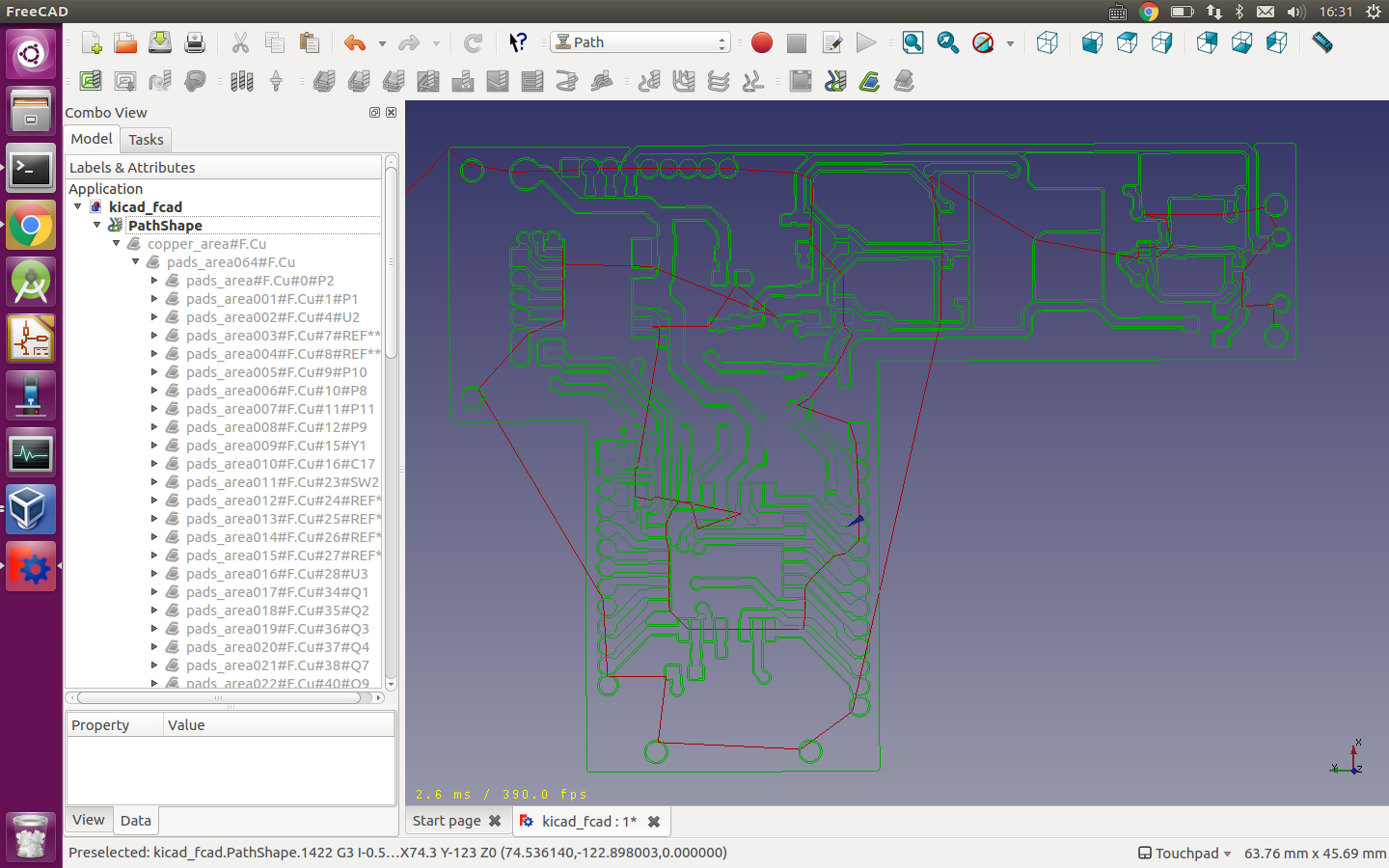
-
- PCB_v2.jpg (225.16 KiB) Viewed 1960 times
Re: PCB design & machining
I think that some people use kicad and export to dxf, than import dxf to Freecad? And really most dont mill all that surface, just router aroud traces, its also beneficial to remove noises from circuit with all that big gnd area.

Re: PCB design & machining
That's great, thank you. Only baby steps so far but learning all the time.
- Attachments
-
- PCB.jpg (97 KiB) Viewed 1781 times

Re: PCB design & machining
This is something I eventually want to try with my machine but have not got around to yet.
The link to realthunder's work looks very useful.
mn00n, what is the smallest tool you are using there, it looks like 1mm straight endmill.
The challenge is on newer ICs which have 0.25mm pads ! Those DIL formats are 70s vintage.
The link to realthunder's work looks very useful.
mn00n, what is the smallest tool you are using there, it looks like 1mm straight endmill.
The challenge is on newer ICs which have 0.25mm pads ! Those DIL formats are 70s vintage.
-
swizzlakalongie

- Posts: 14
- Joined: Wed Feb 10, 2021 5:08 pm
Re: PCB design & machining
The PCB workflow is different to general CAD/CAM. People normally use KiCAD and then export to excellon/gerber files for milling, which is taken care of by another CAM software specific to electronics. It may seem like extra work to have to learn another software, but in the end it's much less work than trying to do this in FreeCAD. At home, i use KiCAD and then FlatCAM to import the gerber files and produce gcode. Inkscape is another possibility if you can get the gcode plugin to work properly. In the industry people tend to use Altium and some other thing for the CAM... some machines can read the gerber files directly.mn00n wrote: ↑Wed Jan 20, 2021 2:59 am Is there an efficient workflow to design a PCB and mill the geometry?
I've been having fun with the latter but started from scratch to create a 3D model, which is pretty laborious.
Happy with the end result, which is great for prototyping, although still learning from each iteration.
Grateful for tips from others that have tried.
-
swizzlakalongie
- Posts: 14
- Joined: Wed Feb 10, 2021 5:08 pm